
Applied Materials and the Angstrom Age
As AI rewires the physics of chip fabrication, Applied Materials posts record quarterly revenue of $7.91 b and raises its full-year outlook to 30%-plus growth, positioning itself as the indispesable


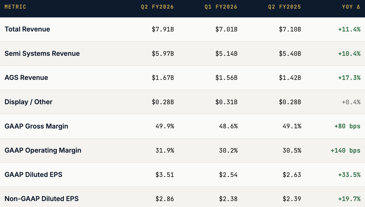
Applied Materials reported record second-quarter fiscal 2026 revenue of $7.91 billion today, beating Wall Street’s consensus of $7.69 billion by roughly $220 million and delivering GAAP earnings per share of $3.51 — a 33% increase year-over-year. The company simultaneously raised its view of wafer fabrication equipment market growth to more than 30% in calendar 2026, up from the “more than 20%” guide issued just three months ago in February. The Q3 fiscal 2026 revenue midpoint of $8.95 billion implies a new quarterly record ahead, underscoring the acceleration of AI-driven capital spending at TSMC, Samsung, SK Hynix, and Micron.
Behind the headline numbers, a structural story is unfolding inside the fabs. Gate-All-Around (GAA) transistors, high-bandwidth memory (HBM) stacks, and advanced packaging workflows — the foundational architectures of next-generation AI accelerators — all demand a materially denser sequence of deposition, etch, and metrology steps. Applied Materials, whose platform portfolio spans each of these disciplines with greater breadth than any single competitor, is uniquely positioned to capture that incremental intensity. Revenue from advanced packaging surged roughly 90% year-over-year, and Cold Field Emission (CFE) eBeam revenue is on pace to cross $1 billion in calendar 2026, doubling in a single year.
The picture is not without friction. China, which accounted for approximately 27% of Q2 revenue, faces accelerating headwinds from U.S. Bureau of Industry and Security (BIS) export restrictions that the company expects to cost it roughly $600 million in fiscal 2026 revenue. A $252.5 million civil penalty — settled with the Department of Commerce over legacy SMIC shipments — has already been absorbed. Management’s posture is that non-China demand is growing fast enough to more than offset the China drag, and the Q3 guide, set above any prior quarter, suggests that math currently holds.
This deep dive reviews Applied Materials’ Q2 FY2026 results in full, dissects its segment economics, maps the AI technology tailwinds reshaping its addressable market, sizes the China risk, and weighs the bull and bear cases for a stock that has compounded at nearly 140% over the past twelve months and trades at a premium to historical norms.
Section 01
Quarterly Results: Records on Multiple Fronts
Applied Materials’ fiscal second quarter, ending April 27, 2026, produced records across virtually every headline financial metric. Revenue of $7.91 billion grew 11.4% year-over-year and exceeded the company’s own guidance midpoint of $7.65 billion by $260 million. GAAP gross margin reached 49.9%, while the non-GAAP figure touched an even 50.0% — a milestone that reflects the sustained mix shift toward high-value leading-edge tools. Operating income on a GAAP basis reached $2.52 billion, good for a 31.9% operating margin. GAAP net income of $2.81 billion translated to diluted EPS of $3.51.
Source: Applied Materials IR filings and LongYield analysis. FY2025 figures estimated where exact actuals unavailable. All figures approximate.
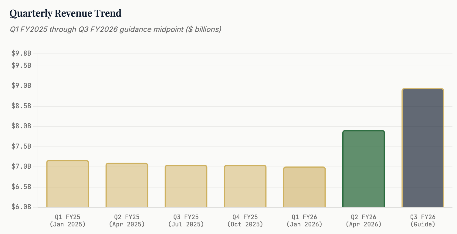
The sequential acceleration from $7.01 billion in Q1 to $7.91 billion in Q2 — a $900 million step-up in a single quarter — reflects both improving mix (more leading-edge tool shipments) and a recovery in fab spending among memory customers. Semiconductor Systems revenue jumped from $5.14 billion to $5.97 billion sequentially, while Applied Global Services continued its methodical climb to $1.67 billion. The guidance midpoint of $8.95 billion for Q3 would represent yet another $1.04 billion sequential jump, suggesting the current upcycle still has significant runway.
Importantly, the company’s gross margin trajectory points toward structural improvement, not merely cyclical luck. CEO Gary Dickerson has repeatedly emphasized that the incremental intensity of leading-edge processes — more deposition films, more etch steps, more metrology touchpoints per wafer — disproportionately benefits Applied’s broad portfolio. Every transistor generation that moves from FinFET to GAA requires roughly 15–20% more process steps, and a meaningful fraction of that incremental work falls within Applied’s addressable domain.
Section 02
Segment Analysis: Three Businesses, One Flywheel
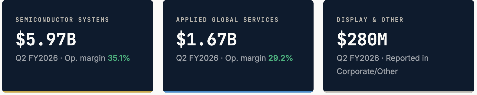
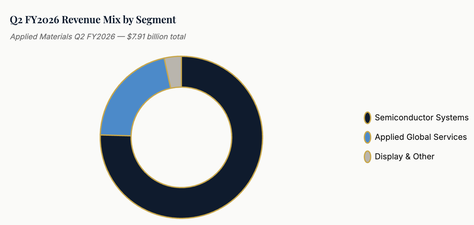
Semiconductor Systems is the engine of the franchise. In Q2 FY2026 it generated $5.97 billion in revenue at a 35.1% operating margin — an expansion of roughly 250 basis points year-over-year. Within the segment, the most notable development is the mix shift toward memory. Foundry/Logic accounted for approximately 67% of Semiconductor Systems revenue, DRAM rose to 29% — up from 27% a year earlier — and Flash (NAND) contributed a modest 4%. The DRAM surge reflects HBM capacity buildouts at SK Hynix, Samsung, and Micron. High-bandwidth memory stacks require dramatically more physical vapor deposition (PVD) and electroplating steps than conventional DRAM, and Applied’s Endura and Centura platforms dominate these workflows. Effective in Q1 FY2026, management consolidated its 200mm equipment business into Semiconductor Systems (previously reported under AGS), increasing segment transparency and reflecting the company’s view that all equipment revenue belongs in a single reportable bucket.
Applied Global Services (AGS) has quietly become one of the most durable businesses in the semiconductor supply chain. At $1.67 billion in Q2 FY2026 revenue — growing more than 15% year-over-year — AGS generates recurring income from a global installed base that now exceeds 55,000 tools, growing at 5%-plus annually. More than two-thirds of AGS revenue comes from subscription-style service contracts rather than transactional parts and labor, a mix that insulates the segment from the capital equipment cycle’s volatility. Operating margin of 29.2% in Q2 expanded by more than 300 basis points from the prior year period, as the leverage inherent in a subscription model accumulates over time. Applied has telegraphed that AGS should grow at a “low-double-digit or better” rate going forward — a forecast anchored by the ever-growing denominator of equipment in the field.
Display, now reported within Corporate and Other, remains a minor and declining contributor. The $280 million in Q2 was roughly flat year-over-year ($279M in Q2 FY2025), reflecting muted investment in OLED and LCD panel capacity. Applied has strategically deemphasized this business, and it no longer warrants a dedicated disclosure segment. The company’s future is categorically tied to the silicon substrate.
Section 03
The AI Tailwind: GAA, HBM, CoWoS, and the Materials Inflection
The semiconductor industry is experiencing what Applied Materials’ leadership calls a structural “materials inflection” — a shift in which the manipulation of atomic-scale materials, rather than optical lithography alone, becomes the primary lever for improving chip performance. This inflection, driven by the scaling demands of AI workloads, plays directly into Applied’s core competencies in deposition, etch, and surface engineering.
Technology Catalyst
CEO Gary Dickerson has stated publicly that global semiconductor revenues could “potentially reach $1 trillion in 2026,” earlier than prior industry forecasts. Applied’s own semiconductor equipment business is guided to grow more than 30% in calendar 2026 — an extraordinary acceleration that reflects the demand density of AI infrastructure buildouts.
Gate-All-Around (GAA) transistors represent the next major architectural leap beyond FinFET structures, and the process transition carries significant implications for equipment intensity. In GAA, gate material wraps entirely around the nanosheet channel, requiring unprecedented precision in atomic-layer deposition (ALD) and selective etch. Applied has introduced multiple tools specifically engineered for GAA: the Viva radical treatment system for nanosheet surface preparation, the Sym3 Z Magnum for angstrom-level conductor etching, and the Spectral ALD system designed to reduce resistance in the tightest junctions. TSMC’s N2 node and Samsung’s 2nm-class processes both rely on GAA, and the tool intensity per wafer at these nodes is estimated to be 15–20% higher than at FinFET nodes.
High-Bandwidth Memory (HBM) has become one of the most consequential secular tailwinds in the current cycle. Each successive HBM generation — HBM3E, and now the emerging HBM4 specification — demands tighter film control in the metal interconnect stack, driving significantly higher utilization of PVD and CVD deposition equipment. In Q2 FY2026, DRAM accounted for 29% of Semiconductor Systems revenue, up from 27% a year ago. Applied’s installed base of Endura PVD systems at the leading HBM manufacturers is extensive, and the company has signaled that its HBM revenue content per wafer has grown by more than 30% over the past two technology generations.
“The fastest-growing packaging segments in 2026 are HBM and 3D chiplet stacking. Applied is exceptionally well-positioned in both.”
— Gary Dickerson, CEO, Applied Materials — Q1 FY2026 Earnings Call, February 2026
Advanced packaging — encompassing CoWoS (Chip-on-Wafer-on-Substrate), Fan-Out Wafer Level Packaging, and 3D chiplet integration — is perhaps the most explosively growing pocket of Applied’s business. Advanced packaging revenue surged roughly 90% year-over-year in fiscal 2025, and 80% of the advanced packaging backlog is tied to HBM interconnect and chiplet integration schemes. To deepen its position, Applied announced an agreement to acquire NEXX, the advanced packaging deposition equipment business of ASMPT Limited. NEXX specializes in large-area panel-level deposition, a technology that allows chipmakers to build physically larger AI accelerators by escaping the constraints of round wafer geometry. The acquisition broadens Applied’s addressable market in the advanced packaging space — one of the highest-growth pockets in the entire WFE landscape.
eBeam metrology has emerged as a $1 billion business in its own right. Applied’s Cold Field Emission (CFE) eBeam platform provides the sub-nanometer measurement capability required to verify pattern fidelity at EUV and High-NA EUV lithography nodes. Management guided CFE eBeam revenue to double in calendar 2026, crossing the $1 billion threshold — a milestone that highlights how the measurement and inspection layer of chip manufacturing is scaling alongside the patterning itself. The VeritySEM 10, Applied’s latest CD-SEM, offers 2x better resolution than conventional systems at lower landing energies, enabling non-destructive characterization of the finest on-wafer structures.
The Centura Sculpta pattern-shaping system rounds out the portfolio discussion. Unlike lithography tools, Sculpta modifies EUV-printed patterns after exposure — elongating resist shapes in a controlled direction to increase pattern density without an additional exposure step. This reduces the cost and environmental footprint of extreme patterning by effectively extracting more usable geometry from a single EUV shot. Chipmakers including TSMC have qualified Sculpta in advanced logic process flows, and the tool exemplifies Applied’s strategy of inserting itself into patterning workflows through materials engineering rather than optics.
Section 04
